I’m building an 8-bit computer capable of running Pong. This post is about the computers’ registers, and other posts in this series are about different stages of building the computer.
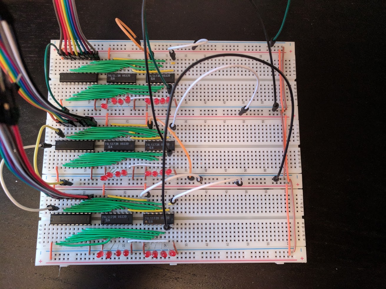
Over the last week, I’ve been building the three data registers of the computer’s CPU. Here’s what they look like. Each row is a separate register with a bus transceiver on the left (so it can write its value to the bus, read from the bus, or not affect the bus at all), and then two 4-bit D flip-flops for storing the data. Eight LEDs on each register will show the current value stored.
The design I’ve based my computer on only had two registers, and I thought I should explain why I’ve added a third to the design.
What is a register?
When a computer runs a programme, the CPU reads code and data from memory (e.g. RAM, but it could also be the hard drive). It interprets the code as instructions, and makes changes to the data depending on what the instructions say. But CPUs can’t interact directly with data in memory - instead they read from memory into registers, change the values in the registers, then write those values back to memory.
One reason for this is speed - registers are very very close to the core of the CPU, right next to the silicon that performs the addition / subtraction / other operations, so they are very fast to work with. Conversely, values in RAM are physically far away, and ever so slow to access.
It’d be great if all your memory could be in registers - then everything would be fast. But registers have to be very small to get close enough to the CPU to be useful. If they were any bigger, they’d have to be further from the core of the CPU, which would make them slower to work with.
Here’s an example where a programme might adds 1 to the number at the address 0x10 in memory. To do that, it will read the number at 0x10 into a register, add 1 to the register, and then write that number back to 0x10. In pseudo-assembly:
LDA 0x10 ; load the value at memory address 0x10 into register A
ADA 0x01 ; add 1 to the value in register A
STA 0x10 ; store the value in register A at memory address 0x10
Why three registers part 1: more variables at the same time.
Because of this design, any time your computer changes data, it needs to use registers.
Registers are also a good place to keep temporary variables. E.g. if your programme has a loop that needs to be executed three times, you could keep the number of iterations that have been performed in a register. If you do any other data operations during the loop, you’ll need either
- a second register to store the data in, or
- to write the loop variable to RAM, use its register for the arithmetic, then read the variable back from RAM when your programme has finished its other data operations.
Having an additional register lets you work with more variables at the same time without having to write them to RAM (which means extra code, and extra clock cycles).
Why three registers part 2: shorter code.
The design I’m building on has its two registers directly joined to the Arithmetic Logic Unit, or ALU (the bit of the CPU that performs the actual maths / logic operations). If your programme subtracts two numbers, the first goes into register A, the second into register B, the ALU is instructed to perform a subtraction, and the result can be read from the ALU’s output.
This is hard-wired - the only way to subtract or add is to put the left-hand side of the operation into register A and the right-hand side into register B.
As well as reducing the number of variables being used at the same time, this
also leads to inefficient code. If you want to add 1 to the value in register A, you first
have to put the value 1 into register B, then you can do the addition. So there’s no way of
doing ADA 0x01 to add 1 to register A in a single instruction - instead you have to write
two instructions.
STB 0x01 ; Store 1 in register B
AAB      ; Add the values in A & B, store the result in A
Taking 2 instructions rather than one would normally not seem like a significant problem in a programme, but I have a tight limit to fit the code of the game into (256 bytes), so every instruction matters.
A third register lets me have more variables in use at the same time, and
lets me keep a register exclusively for arithmetic, which won’t be directly
used in any instructions of the programme. Then I can still have a hard-wired ALU
between registers A & C, but I can create shorter instructions like ADA 0x01
without worrying about overwriting programme data in registers.
A digression on buses
While thinking about this problem, I realised that a proper CPU would almost certainly let any register or value be the operands for its sums and logic.
That’s difficult to achieve when your ALU is hard-wired between two registers, so I imagine it’s done by using additional buses. In my computer, there’s a single bus connecting everything, and the computer controls which components are reading and writing to the bus.
A high-end CPU probably has separate buses for each of the operands to the ALU. Then to subtract between any two registers, you’d design the CPU to write one register to the bus for the first operand, and the other register to the bus for the second operand, and the ALU would then be able to take its inputs from any part of the CPU.
I’m not going to go to that level of design - buses take up a lot of space on breadboards - but it might be a fun extension to this project later, or an option to use if I can’t get my Pong code small enough to fit into memory, or fast enough to be playable.
What’s next?
Now that the registers are built, I’m next going to build the ALU to go between two of them.