I’m amazed to find it’s been 8 months since my last update. I’ve clearly been busy.
The ALU and status register are broadly working, but I was getting some odd behaviour when I tried to connect everything up - the clock was gradually slowing down, and I was seeing an in-between logic level in some places - neither a 1 or 0.
My best guess at the moment is that the problem is because I hadn’t fully wired up every control signal, and there was probably a short between +ve and ground somewhere, for example if two chips were outputting to the bus at the same time, and one had a 1 and the other a 0.
Rather than try to deal with the mess of wires and connect everything up fully, I’m going to build more of the control systems, test those, connect everything up, and then debug the other components when they’re fully connected.
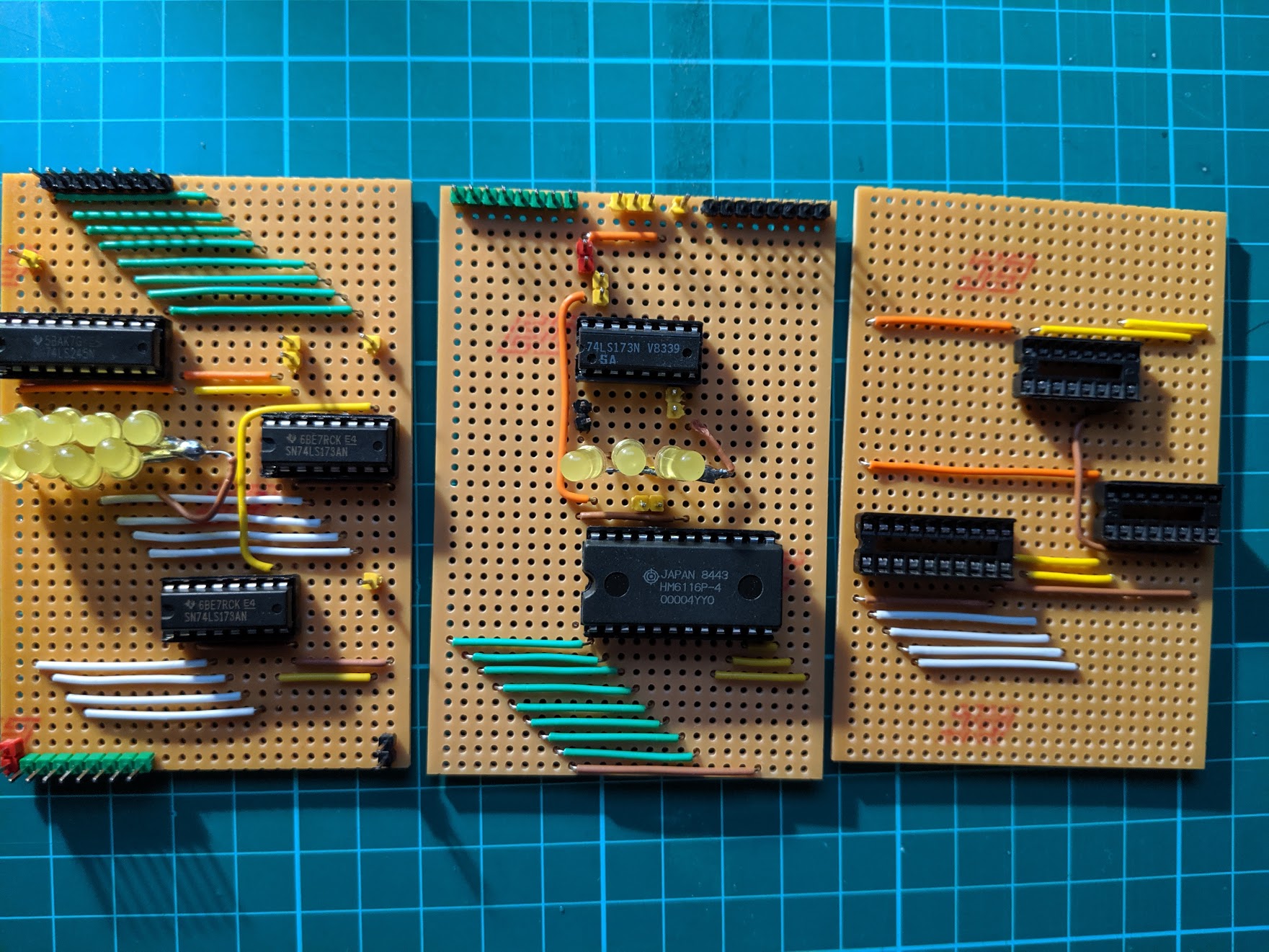
I’ve now designed the RAM circuit boards and built them. The RAM chip I’m using has an 11-bit address space, so I’ve added an extra little register to select the “3-bit bank” of RAM. That’s not quite as good as using 11-bit addresses (changing between banks of RAM will need extra instructions), but it could still prove useful for programs that need more than 256 bytes of RAM. That also meant adding a control signal for “set RAM bank”.
I’ve also designed a Program Counter and started building it. It’s pretty straightforward - an 8-bit register that can read its contents from the bus, but can also increment its value by 1.
I’m also going to adapt the existing boards to try to avoid such a mess of wires. To do that, I’m adding two jumpers everywhere I previously had one. That means for shared lines, like +ve, 0V, clock, reset, etc., I can connect board-to-board rather than connecting every board to the same common rails. That should make the finished computer tidier, and make testing easier.
If you’re interested you can see the schematics in the Github repository.
